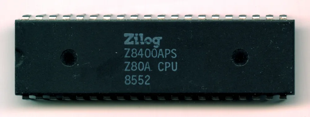
There’s a Z80A on the bench in front of me right now, prised out of a dead Amstrad CPC464 that spent the better part of a decade in a leaking garden shed. The Zilog Z80A is an 8-bit microprocessor, the 4 MHz revision of the Z80 that Zilog launched in July 1976, and for the better part of two decades it was probably the most common processor on the planet outside a mainframe room. It ran the Sinclair ZX Spectrum, most of the Amstrad CPC range, every machine built to the MSX standard, a huge slab of arcade hardware and the entire CP/M business-computing world. Zilog only stopped making it in 2024.
- Manufacturer: Zilog, designed by Federico Faggin, Masatoshi Shima and Ralph Ungermann
- Launched: July 1976 (original Z80); the 4 MHz Z80A followed within the year
- Clock speed: 4 MHz, up from 2.5 MHz on the original Z80 and eventually up to 20 MHz on later CMOS revisions
- Bus width: 8-bit data bus, 16-bit address bus, giving 64KB of directly addressable memory
- Power and package: single 5V rail, 40-pin DIP, no external clock generator or bus controller needed
- Discontinued: standalone DIP parts withdrawn in June 2024, 48 years after launch


Left: Image source unknown. If this is your picture, contact us and we’ll credit or remove it. Right: Image source unknown. If this is your picture, contact us and we’ll credit or remove it.
Federico Faggin and Ralph Ungermann
Two engineers, an oil company and a grudge against Intel
Federico Faggin and Ralph Ungermann walked out of Intel in late 1974, tired of losing internal battles over how the company should build its next microprocessor. Masatoshi Shima, who had done the transistor-level logic design on both the Intel 4004 and the 8080, joined them in April 1975. Together they founded Zilog and started work on a chip they called, with the sort of confidence only a founder can muster, the Super 80.
They needed money before they needed a name that stuck, and by April 1975 they had a verbal commitment for $500,000 from Exxon Enterprises, the oil giant’s venture arm. So the processor that ended up inside the ZX Spectrum was funded, in part, by Exxon.
A few years later that backing came back to bite. Zilog’s follow-up 16-bit chip, the Z8000, was a genuinely capable design. According to Faggin and Shima’s own account at a 2007 oral history panel at the Computer History Museum, IBM rejected it outright for the machine that became the IBM PC, and the reason had nothing to do with the silicon itself. Exxon was aggressively expanding into the computing business at the time, and IBM wanted no part of building its flagship product around a chip controlled by a company it viewed as a direct competitor. The Z80A’s own funding arguably cost its successor the biggest design win in personal computing.
What made switching from an 8080 worth the redesign
The Z80 was designed to run existing Intel 8080 object code without modification, which meant every CP/M program already on the market worked on Z80 hardware unchanged. That single decision let Zilog sell into an installed base rather than build one from nothing.
Everything else Zilog added on top of that compatibility answered a specific 8080 complaint. The 8080 needed three separate voltage rails, plus 5V, minus 5V and plus 12V, and two support chips just to function: the 8224 clock generator and the 8228 bus controller. The Z80 folded both of those functions onto the CPU die itself and ran from a single 5V supply, so a Z80-based board needed fewer components and fewer things that could fail on a hobbyist’s breadboard. The register count doubled too, with a complete shadow set (AF’, BC’, DE’, HL’) a programmer could swap in with a single instruction, invaluable for fast interrupt handling, where saving and restoring registers the slow way could cost more cycles than the interrupt routine itself. Block-move instructions like LDIR did in one instruction what the 8080 needed a hand-written loop to achieve. None of it was flashy, but all of it made a board cheaper to build.
A four-bit heart doing eight-bit sums
Pull back the metal lid, or more realistically, read Ken Shirriff’s die analysis rather than turn a working chip into scrap on your own bench, and the Z80 keeps a secret that never once leaked into a datasheet. Its arithmetic logic unit is only four bits wide. Every 8-bit ALU operation the instruction set claims to do in a single pass is actually done in two consecutive internal clock cycles, four bits at a time, with the result stitched back together before anything downstream notices. A programmer counting cycles from Zilog’s own timing tables never sees this. The abstraction holds perfectly. The hardware underneath is doing twice the work the manual implies.
The program counter gets the opposite treatment: a dedicated 16-bit increment and decrement circuit with carry-lookahead and carry-skip logic, built purely for speed, because the PC gets touched on essentially every instruction fetch and a slow increment there would have throttled the whole chip. Zilog’s designers spent silicon lavishly on the one thing that ran constantly and stayed miserly everywhere else.
Why the data pins look wired by someone in a hurry
Trace the data bus on a Z80A with a multimeter and a schematic and you’ll start doubting your own continuity readings. The eight data pins don’t run D0 through D7 in order around the package. They run D4, D3, D5, D6, D2, D7, D0, D1, a sequence that looks less like engineering and more like something typed in by someone who’d had one coffee too many.
It isn’t a mistake. Ken Shirriff’s 2014 analysis of the die photographs settled the question: the Z80’s internal data bus is split into segments so the chip can do several things with it at once, reading an instruction byte off the pins while simultaneously shuffling data between the ALU and the register file on a different segment entirely. The pin order simply follows where each segment happens to land at the edge of the die. Shrinking the die to tidy the pinout up would also have cost Mostek, Zilog’s foundry partner, real money on every wafer, which made the ugly layout an easy trade to accept once the parallelism was already the point. Nobody outside Zilog noticed for thirty-eight years.
Static versus dynamic: the difference between paused and dead
The original NMOS Z80 and Z80A use dynamic logic internally: certain states are held as a charge on parasitic capacitance rather than in a proper latch, which is cheaper to build but means that charge leaks away if the clock stops or runs too slowly. Slow the clock down too far on an NMOS Z80A and it doesn’t pause gracefully. It just forgets what it was doing. The later CMOS parts, the Z84C00 family, are fully static and hold state indefinitely with the clock stopped dead, which is why every hobbyist single-stepping a Z80 by hand with a manual clock generator is quietly relying on a CMOS chip, not the museum-piece NMOS original. Most repair guides skate past this, and at the bench it matters.
More often, a Z80A that freezes, miscounts or locks up mid-boot on the bench has a missing or degraded 0.1 µF decoupling capacitor between pin 11 and pin 29 (the 5V rail and ground), starving the chip of a clean supply the instant it needs to switch. A logic probe earns its keep here. BUSRQ should sit high at rest. IORQ is active-low and pulses only when the chip is actually addressing a peripheral, while INT shows genuine high-low activity rather than sitting stuck. If the address or data lines wander unpredictably between rail voltages on a scope trace, that’s usually tristating, the bus doing exactly what a bus does when nothing is driving it.
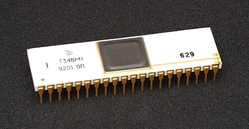
Photo: Konstantin Lanzet, Wikimedia Commons (CC BY-SA 3.0)
The instructions Zilog never admitted existed
Buried inside the Z80’s opcode map are instructions the official documentation never mentions, because Zilog never intended them to be used. The undocumented set lets a programmer address the high and low bytes of the IX and IY index registers directly, as IXH, IXL, IYH and IYL, as if they were ordinary 8-bit registers rather than halves of a 16-bit pair. Zilog never guaranteed they would behave this way on future silicon. Game developers used them anyway, extensively, because shaving a handful of cycles off a tight interrupt routine mattered more than a guarantee from a chip manufacturer nobody expected to still be reading datasheets in five years’ time.
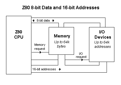
Image source unknown. If this is your picture, contact us and we’ll credit or remove it.
The same undocumented territory holds a small trap for anyone assuming NMOS and CMOS parts are interchangeable: the unofficial OUT (C), 0 instruction outputs 0xFF on NMOS silicon and 0x00 on CMOS silicon. That single bit of difference has broken exactly nothing in properly written software and exactly everything in software that leaned on it. National Semiconductor found this out the hard way with the NSC800, its own Z80-compatible part. A different pinout and a different interrupt structure meant it diverged from some of this undocumented behaviour, and games built around the genuine article simply refused to run correctly on it.
One processor, a hundred machines
At around $25 a chip, the Z80A undercut the Intel 8080 badly enough to make an entire generation of affordable home computers possible: the Sinclair ZX Spectrum, the Amstrad CPC range, the MSX standard in its entirety, a long list of CP/M business computers and enough arcade boards that a working knowledge of Z80 assembly was, for a while, simply part of being a games programmer.
The clone lineage the West rarely credits
The Z80’s reach went well beyond machines built under licence. Behind the Iron Curtain, VEB Mikroelektronik in Erfurt, East Germany, built the U880, an unlicensed NMOS copy of the Z80 that powered a huge share of Eastern Bloc computing, reverse-engineered and manufactured without Zilog seeing a single mark of royalty. The Soviet Union followed with its own NMOS and CMOS equivalents, the KR1858VM1 and KR1858VM3. Building a working, pin-compatible copy of a Z80 from scratch, under a trade embargo, with a domestic fabrication process years behind Mostek’s, took serious reverse-engineering skill in its own right. The engineers who managed it deserve the same respect as the ones who wrote the original ALU logic, whichever side of a border they happened to work on.
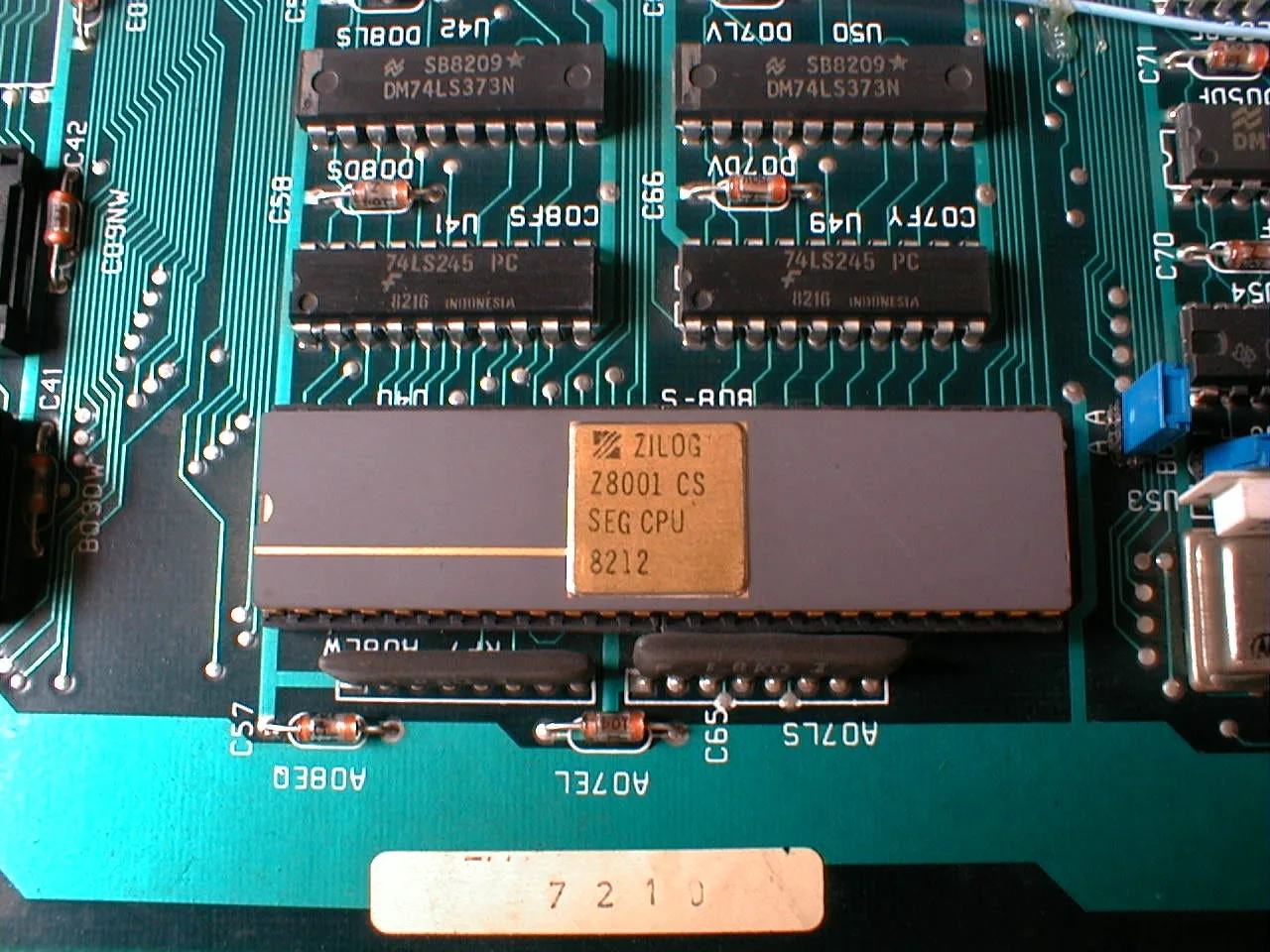
Image source unknown. If this is your picture, contact us and we’ll credit or remove it.
Licensed second-sourcing told a calmer version of the same story. NEC’s µPD780C shipped as a straightforward compatible part, while National Semiconductor’s NSC800, already discussed above, showed what happens when ‘compatible’ quietly stops meaning what everyone assumed it meant.
Forty-eight years, then a last-time-buy notice
Zilog’s end-of-life notice for the standalone Z84C00 family is dated 15 April 2024. Last-time-buy orders closed on 14 June 2024, putting the standalone Z80’s working life at just under forty-eight years from its July 1976 launch, longer than the careers of most of the engineers who designed it. The eZ80 embedded core keeps the architecture alive inside industrial and automotive silicon that will outlive most of us. What ended in 2024 was just the last-time-buy notice on a bare 40-pin part nobody had put into a new design for years anyway.
The Z80A outlasted the Intel 8080 it was built to beat, Zilog’s own Z8000 that was meant to replace it, and Exxon Enterprises, the oil money that funded it into existence. Whatever’s on the bench in front of you when you finally get that dead Amstrad running again, there’s a reasonable chance it’s still the same processor, doing the same four-bit trick, forty-eight years on. Not bad for a chip nobody bothered giving a proper pinout diagram.